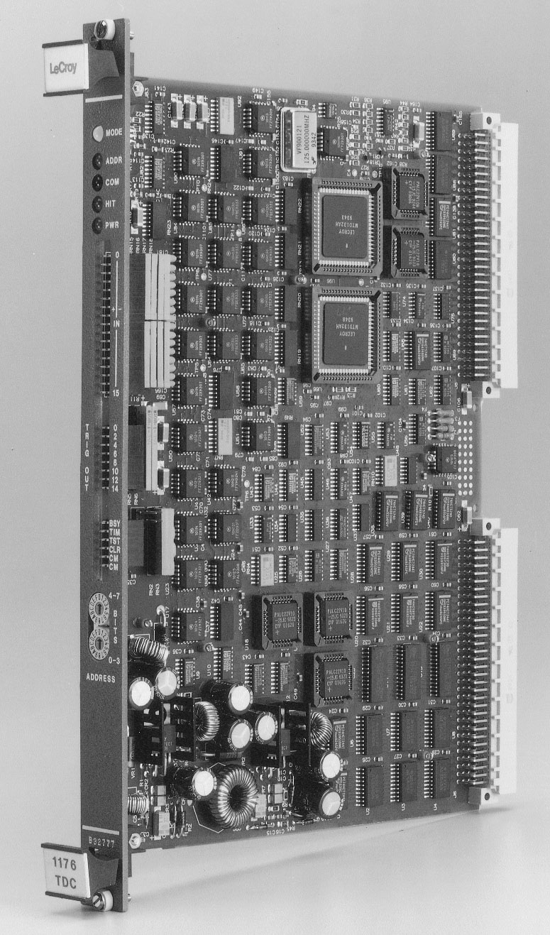
1176 Multihit Time-to-Digital Converter |
|
The 16-channel, VME Model 1176 Multihit Time-to-Digital Converter (TDC) has been
designed for high rate environments. The module features a 16-bit dynamic range and 1 nsec
LSB, 750 psec R.M.S. The double edge resolution is below 20 nsec. The module is ideal for
time measurements of drift chambers, time projection chambers or other detectors requiring
time interval measurements with high accuracy.
The Model 1176 can be operated in either a Common Stop or Common Start mode. At the end of
the acquisition period, the time elapsed between each hit and the Common Stop or Start
along with the address of the associated channel is made available for readout. Readout is
via standard VME, and the data are automatically zero sup pressed. A trigger port with
prompt outputs is also provided.
The Model 1176 is based on the MTD132A, an application specific integrated circuit,
which is an 8-channel, 16-bit dynamic range TDC circuit with 1 nsec least count. Arrival
times can be recorded for the rising edges, the falling or both edges.
The COMMON input located on the front panel accepts standard ECL signals and has jumper
connected, 110 ohm terminating resistors. By removing these jumpers the common signal can
be daisy chained to several 1176 modules, as long as the last terminating resistors are
left connected. This scheme eliminates the extra propagation delays caused by embedded
repeaters and leaves only the very slight delays due to the cables (approxi mately 50
psec/cm).
Buffering time depends on the number of hits recorded. VME readout may start after
buffering ends. The 1176 supports block transfer for faster readout.
An on-board tester delivers hits to all channels for functional verification. The number
of hits and pulse width are programmable. A test cycle is initiated by writing to CSR0.
Prompt hit information is presented to an ECL auxiliary port for inclusion in first level
trigger decisions. These prompt signals are compatible with the LeCroy ECLine series of
logic units.
By capturing both the leading and trailing edge time information, the 1176 can be used
in a "time-over-threshold" technique to simultaneously determine the time and
total charge collected (or, in some cases the time and peak value) for a given detector
element using only one channel of TDC electronics. This technique avoids many of the
traditional problems encountered with other methods, such as amplitude saturation, at a
greatly reduced cost.
VME CONTROL
VME Device Type: A24/D32/D16/D8 (EO) Slave.
Base Address: Front-panel switch selectable, A16-A23.
Address Modifier Codes: AM = 39, 3B, 3D, 3F.
DTACK: On valid address and no internal error.
GENERAL
Channels: 16, differential ECL inputs. Impedance 112 ohm. Unused inputs/outputs are
allowed to float.
Common Start/Stop: Front panel ECL 2-pin connectors; 110 W jumpered terminating
resistors.
Multi-Event Buffer: 32 events (the last hit in an event is marked by Bit 23 = 0).
Range: 16 bits.
Full Scale: 65.536 �sec.
Least Significant Bit (LSB): 1 nsec.
Double Edge Resolution: The MTD132A can measure two dissimilar edges separated by
as little as 20 nsec. Edges of the same polarity must be no closer than 40 nsec. This
implies a double pulse resolution of 40 nsec.
Long Term Stability: 10 ppm/year.
Integral Non-Linearity: 10 ppm.
Differential Non-Linearity: �0.2 LSB maximum.
Channel-to-Channel Pedestal: < �1 nsec.
Total R.M.S. Error: < 750 psec. (Note: The R.M.S. of a Gaussian distribution is
equal to sigma.)
Fast Clear Response: Differential ECL input via a 2-pin front-panel connector
(removable termination resistors) or via Bit 32 in CSR. Minimum pulse width is 20 nsec.
Fast Clear can be applied at any time after a common in put. Fast Clear stops and clears
the current event and readies the module for acceptance of a new event. Fast Clear setting
time is less than 200 nsec from the leading edge of fast clear input.
Fast Clear Window (FCW): Starts at end of Time Range (Common Start) or at Common
Stop. Can be programmed via CSR between 1 �sec and 128 �sec. During this period, the
user can apply a FAST CLEAR to dis card the event just captured.
Multiple Event Buffer: The digital data memory is logically organized as a FIFO,
large enough to store the re sults of up to 32 events. A 5-bit event counter allows the
user to keep track of how many events the readout is trailing the triggers.
Internal Tester: Even channels and/or odd channels may be tested. The tester
generates square ware pulses (50% duty cycle). The pulse trains can have 1, 2, 4 or 8
cycles with half periods of 62.5, 125, 500, or 1000 nsec.
Buffering: 1.25 �sec + 125 nsec per hit.
Readout: VME readout can begin after Buffering in Progress is false and can
continue at full VME speed.
Data Format: 16 bits data, 1 bit edge polarity, 4 bits channel address, 1 validity,
1 end of event.
Packaging: 6 U x 160 mm, single-width VME module in conformance with VME
Specification (ANS/IEEE -1014C).
FRONT PANEL LEDs
MODE: Bicolor LED indicates COMMON START/STOP.
ADDRESS: Yellow LED indicates VME address to module.
HIT: Green LED indicates whether any channel received a hit.
COMMON: Red LED indicates whether a COMMON START/STOP was received.
DIFFERENTIAL ECL SIGNALS
IN: Hit Inputs; 16 channels.
TRIG OUT: Fast Trigger Outputs; 8 outputs - pairwise OR'd channels.
BSY: Busy Output; indicates front end disabled due to buffering, acquisition
disabled or module is full.
TIM: Timeout Input; determines Common Start acquisition window when enabled.
TST: Test Input; provides test pulses to the odd or even numbered channels, as
programmed.
CLR: Clear Input; resets module - aborts conversion.
CM: Common Start/Stop Input; 2 bridged connectors.
Allocation of Address Space
0x0000 to 0x03FF: Event 0
0x0400 to 0x07FF: Event 1
.
.
.
0x7C00 to 0x7FFF: Event 31
0x8000 to 0x8003: CSR
Copyright� July 1997. LeCroy is a registered trademark of LeCroy Corporation. All rights reserved. Information in this publicaction supersedes all earlier versions.