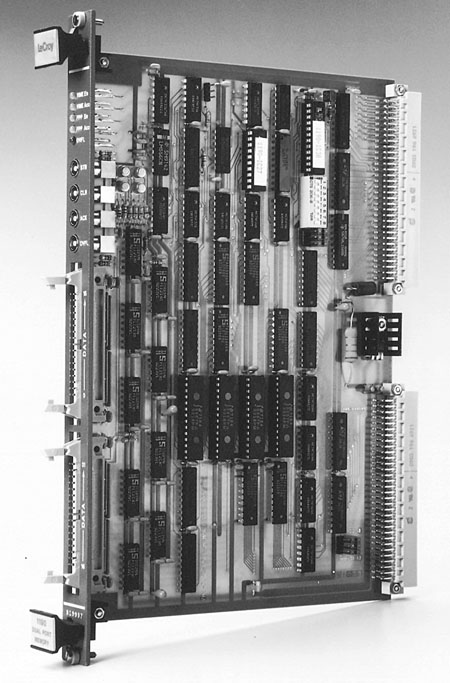
1190 VME DUAL PORT MEMORY |
|
The 1190 Dual Port Memory is a VME memory module (6U) available with 128 kB (32K words)
of data storage. The memory can be loaded via the VME backplane with either D16 or D32
commands or via the 32-bit front panel port (FPP). The memory has an address counter and
is optimized for high speed block transfers with the D32 command. Address pipelining is
not supported.
Since there is only one address counter, the two ports cannot be used simultaneously. The
active port is enabled by a mode bit. For diagnostic purposes, the VME port can be
permanently enabled via an internal jumper.
The front panel port accepts 32-bit data with a strobe (STRobe). The input signals are
complementary ECL. This input format is compatible with the LeCroy ECLine standard input.
Data rates of up to 64 MB/sec can be attained.
The main purpose of 1190 memory is to provide a data sink for the LeCroy ECLbus, such as
the FERA ADC System, the PCOS III Multiwire Proportional System, and FASTBUS via the 1821
Master (see separate data sheets for more details). As such, it acts as a uni-directional
buffer between various standards such as CAMAC (IEEE-583) and FASTBUS (IEEE-960-1986).
INPUT
Data Inputs: 2 front-panel 34-pin connectors which accept complementary ECL signals;
100 ohm input imped ance; 32 parallel bits can be accepted and stored in the memory word
addressed at the strobe pulse arrival time; the memory address is automatically
incremented by one at the end of the strobe pulse. The data must arrive within 5 nsec of
the STRobe and remain valid for at least 25 nsec.
Write Strobe (STRobe): NIM: one Lemo-type front-panel connector with 50 ohm
impedance; accepts a NIM level pulse with a minimum width of 10 nsec. ECL: located on pins
33 and 34 of the upper 34-pin connector (DATA 0 - 15); the connector accepts a
complementary ECL pulse with width of at least 10 nsec and 100 ohm input impedance. The
leading edge of the strobe pulse must fall inside the data pulse and must arrive within 5
nsec; maximum frequency 15 MHz.
Clear (CLR): NIM: One front-panel lemo-type connector with 50 ohm impedance;
accepts a NIM-level pulse with a pulse width of at least 10 nsec; resets the address
counter.
OUTPUT
Acknowledge (ACK): NIM: front-panel Lemo-type connector, outputs NIM level pulses,
minimum width 25 nsec. ECL: located on pins 33 and 34 of the lower 34-pin connector (DATA
16 - 31); the connector outputs a complementary ECL pulse with width of at least 25 nsec
output suitable to drive 100 ohm lines.
Overflow (OV): NIM: front-panel Lemo-type connector, outputs NIM level pulses,
minimum width 25 nsec.
GENERAL
Packaging: 6 U x 160 mm, single-width VME, in conformance with VME specification
(ANSI/IEEE-1014C).
Operating Temperature: 10 to 50 C.
Storage Temperature: -30 to 85 C.
Maximum Humidity: 80% non-condensing at 30 C.
Power: +5 V at 1100 mA; -12 V at 500 mA.
TIMING
VME ACCESS time is measured as DS0/1 to DTACK. Table 1 shows typical times for various VME
operations.
Table 1
FRONT-PANEL LEDs
VME Enabled: Displays that the mode register is set to "FPP DISABLED" or
that the jumper W2 is "on" and W1 is set "off".
VME Access: Displays that an allowed access is being performed, and that the module
is generating DTACK.
FP Enabled: Displays that the mode register is set to FRONT PANEL ENABLED. Note
that the FFP may be disabled because of an OVERFLOW.
FP Access: Displays that a successful access via the Front Panel Port.
OVFL: Displays that the memory address counter has exceeded the existing memory
area.
Designed by the University of Freiburg, Germany.
Copyright© September 1995. LeCroy is a registered trademark of LeCroy
Corporation. All rights reserved. Information in this publicaction supersedes all earlier
versions.